Quick answer
Zynq XADC tutorial, Part 2: The HW design is an open source FPGA project from Hackster.io, indexed by ZouIC. Tutorial on how to use Xilinx Zynq-7000 XADC. Part 2 of 3 explains how to do the HW design in AMD Xilinx Vivado.
- Source
- Hackster.io
- Focus
- FPGA
- Author
- Viktor Nikolov
- Published
- 2024-10-27
Common questions
What does Zynq XADC tutorial, Part 2: The HW design do?
Tutorial on how to use Xilinx Zynq-7000 XADC. Part 2 of 3 explains how to do the HW design in AMD Xilinx Vivado.
Where does Zynq XADC tutorial, Part 2: The HW design come from?
ZouIC indexes it from Hackster.io, original page at https://www.hackster.io/vnikolov/zynq-xadc-tutorial-part-2-the-hw-design-f00cb1.
What stack does Zynq XADC tutorial, Part 2: The HW design use?
tags AMD Xilinx, protip, advanced.
When was Zynq XADC tutorial, Part 2: The HW design published?
The source page lists 2024-10-27.
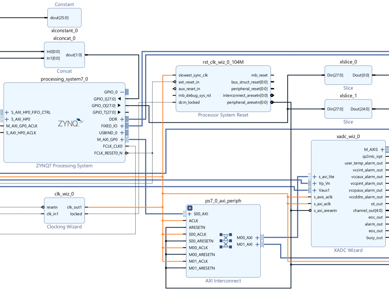
Indexed by ZouIC from the source platform public page, for developer reference only. Copyright and licensing stay with the author; get code and files from the original platform.
Zynq XADC tutorial, Part 2: The HW design
Published 2024-10-27
Tutorial on how to use Xilinx Zynq-7000 XADC. Part 2 of 3 explains how to do the HW design in AMD Xilinx Vivado.
Technical Specifications
Related resources and purchase links
Statistics
Similar Hardware Projects
Project Info
Author Info
Related Links
Keep exploring
Citation Note
This content is sourced from Hackster.io Platform,All rights reserved by the original author. This platform only provides indexing and summaries. For detailed content, please visit the original link.